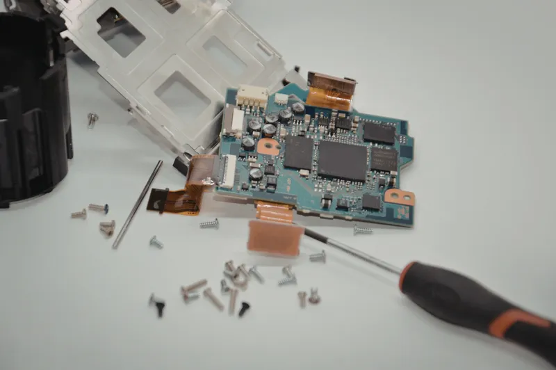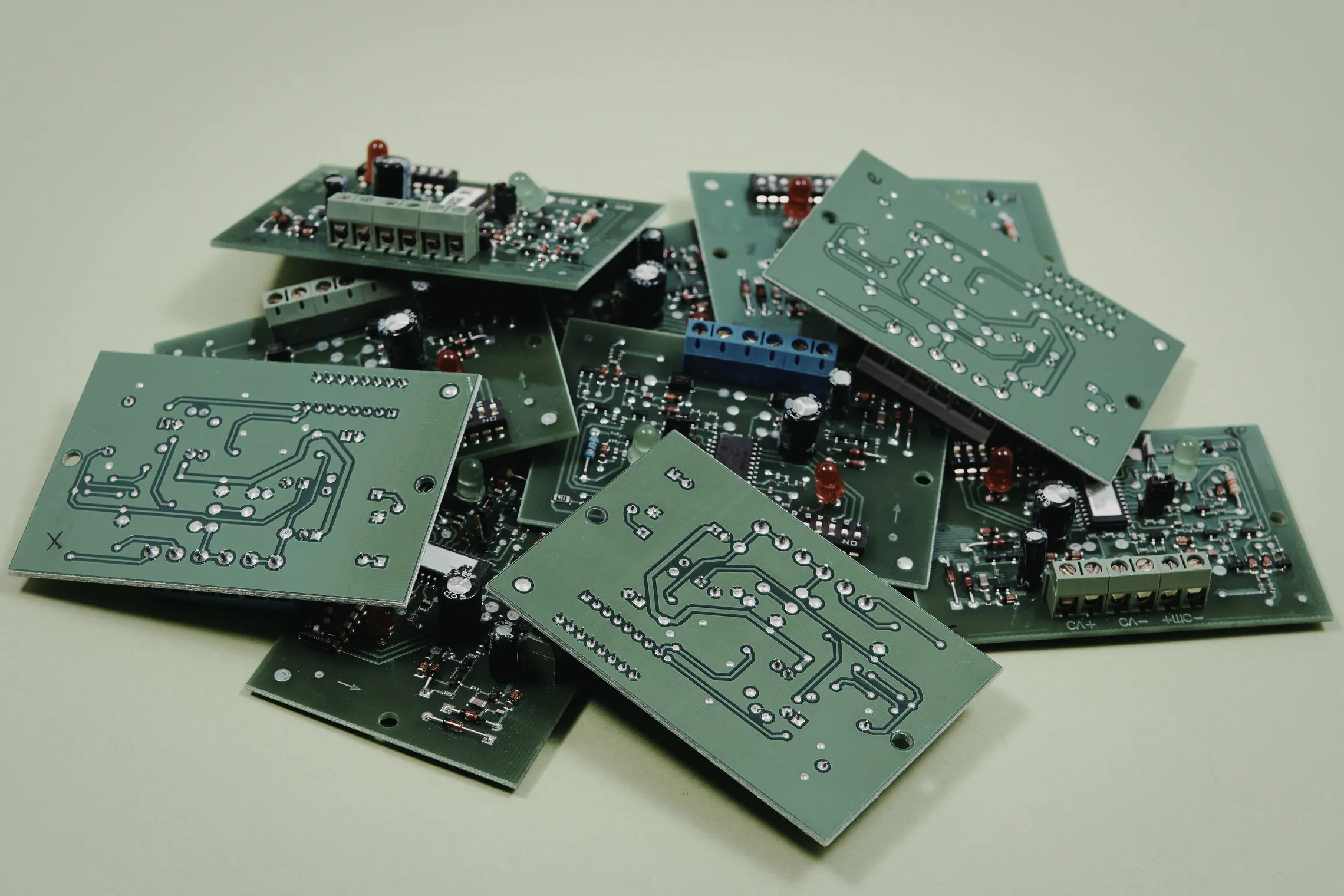
Last July, during the bring-up of one of our prototypes, a daughterboard hand-soldered to its carrier through castellated pads powered up first time: correct current draw, supply rails and analog inputs exactly as designed. Yet the I2C clock line stayed low against its pull-up resistors, and the small memory that identifies the board did not answer: solder defects, fixed by reflowing four pads. The same week, two out of five daughterboards of another type did not answer on the identification bus when first fitted. Their memory comes in a leadless package with the pads under the body, where a cold joint is invisible. A “does it power up?” check would have passed every one of them.
We located the faults without touching the board with a probe. Over the SWD debug interface we read the microcontroller pin level, then reconfigured the same pin as an input with a pull-up and read it again: that is enough to tell a short from an open. It is a hand-made version of what boundary scan does systematically – using the devices' own logic to test connections where probes cannot reach.
That board was badly built and powered up fine. When an OEM moves a board into production, usually at a contract manufacturer, the test strategy is one of the first questions on the table – and these two questions tend to get mixed up: is the board built correctly? and does the board do its job? In-circuit test (ICT), flying probe and boundary scan answer the first; functional test answers the second. ICT vs functional test is not a contest with a winner: none of the four methods replaces the others, and the right mix depends on what you need to catch, on volume and on how the board was designed.
ICT, flying probe and boundary scan look for manufacturing defects: a wrong part, an open solder joint, a short. Functional test proves that the board works when powered, firmware included. Almost every product in series production combines more than one.
In-circuit test (ICT): the bed of nails
ICT uses a dedicated fixture, the bed of nails: a plate of spring-loaded pins that, once closed on the board, touches every test point at the same time. The tester measures components one by one – resistors, capacitors, diodes – and looks for shorts and opens, largely with the board unpowered.
- Strengths: once the fixture exists, testing each board is fast, and diagnosis is precise: it points at the faulty part or net.
- Limits: the fixture is product-specific, costs money and takes time to build; every net to be tested needs an accessible test point, and a layout revision can mean reworking the fixture.
- Use it for: stable designs and production volumes that pay back the fixture.
A bed of nails, though, is a way of contacting the board, not a test method. For a bed-of-nails station we built recently, the request said “ICT”; what was actually needed was to power the board, program it and check that it works through the pins, with no component-level measurements. The same project was a reminder of two practical rules: a test point too close to a tall component cannot be reached, and has to be moved at design time or dropped; and a pin that does not seat properly on its pad looks exactly like a board fault until the fixture is adjusted.
Flying probe: fixtureless testing
In a flying probe tester the probes ride on motorized axes and touch test points one after another, following a program generated from the board's design data. The measurements are largely the same as ICT, with no dedicated fixture to build.
- Strengths: no fixture, so low start-up time and cost; a new revision means updating the program, not rebuilding hardware.
- Limits: the probes move point by point, so each board takes longer than on a bed of nails.
- Use it for: prototypes and NPI (new product introduction), small batches, products with many variants or frequent revisions.
Boundary scan: where probes cannot reach
Boundary scan is standardized as IEEE 1149.1 and widely known as JTAG after the Joint Test Action Group, the group of semiconductor manufacturers whose recommendations became the basis of the standard. It uses test logic built into compliant devices: a chain of cells at the pins, controlled through a test access port (TAP) with four signals – TCK, TMS, TDI and TDO – plus an optional TRST. Driving the pins from inside the devices tests interconnections even where no probe can reach, for example under a BGA.
The same access is often used for programming and debug, but it is not the rule: many products load their firmware through a bootloader, over USB (DFU) or CAN. On the board behind that bed-of-nails station, the full JTAG port is brought out to test points, yet the product is programmed over USB and the test never uses JTAG: the pads serve only as SWD, the two-wire debug interface of ARM cores, for diagnosis.
- Strengths: coverage of nets with no physical access, no complex fixture, well suited to dense boards.
- Limits: covers only nets connected to devices that implement the standard, and the JTAG chain has to be in the schematic.
- Use it for: boards with BGAs, microcontrollers, FPGAs or processors, and little room for test points.
Functional test: the board at work
Functional test powers the board and puts it to work: it drives the inputs, measures the outputs, talks on buses such as CAN or serial, and checks voltages, currents and timing against defined limits. It catches what the other methods cannot see: wrong firmware, analog performance out of tolerance, dynamic behavior that only shows up with the board running. It is also the only test that exercises the board the way the customer will use it.
It needs an interface fixture, measurement instruments and software that runs the sequence and records results by serial number. In production it is typically the end-of-line test, and its cost grows with volume for as long as it stays manual.
How to combine them
The mix depends mostly on the product's stage and on volume:
- Prototypes and first builds: flying probe for assembly defects and functional test, even manual, to validate the design.
- Stable production at medium to high volume: ICT or boundary scan for manufacturing defects, automated functional test at end of line.
- Dense boards with BGAs and little room for test points: boundary scan in place of much of the ICT, plus functional test.
In every scenario functional test stays: structural methods tell you the board is assembled as designed, not that the design works.
Ask for coverage, not just the method
“We run ICT” does not say how much of the board is actually verified. The figure that matters is test coverage: which components and nets each method checks, and which it leaves uncovered. Ask your contract manufacturer or test supplier for it, method by method: the gaps of one method are what the other has to cover, and a defect that neither of them sees ships to the customer. In the case at the top of this article, functional test found the faults because it exercised that very bus: a net that no test exercises is a net nobody has checked.
The test strategy is decided at design time
Accessible test points, a JTAG chain reachable from a connector, an interface for the functional fixture: these are DFT (design for testability) choices that cost little while the board is being drawn and a lot once the layout is frozen. On our microcontroller boards we routinely place a programming footprint for a spring-pin cable, Tag-Connect style, with no connector fitted: it serves production and field service and adds nothing to the BOM. Where we can, the test runs over the bus: the board reports its own supply voltages, temperatures and diagnostics over CANopen, so a production bench needs only the bus and power. Where the board has test points, the fixture reaches them with pogo pins. That is why the test strategy belongs in electronic design from day one, agreed with whoever will manufacture the product – a point worth settling early when the contract manufacturer and the design partner are in different countries.
There is no single best test method: there is the right mix for a board, a volume and a product stage. If you are defining the test strategy for a new board or reviewing the current one, see how we approach testing and inspection or get in touch: we start from the schematic and the volumes you plan to build.