
Encoder read and powered over a single field cable, up to ~100 m at ≤ 1 MHz
NEXOR DAUGHTERBOARD · INTERFACE
Bliss SSI interface for absolute encoders and sensors
Bliss is the SSI interface daughterboard for the Nexor carrier. It gives the node a differential RS-422 link to an absolute encoder or an SSI-output transducer, and powers that device over the same field cable. The sensor needs no local supply: a single cable runs from the node out to the machine.
Solders onto the Nexor carrier: power, processing and CAN are already on board. Discover the platform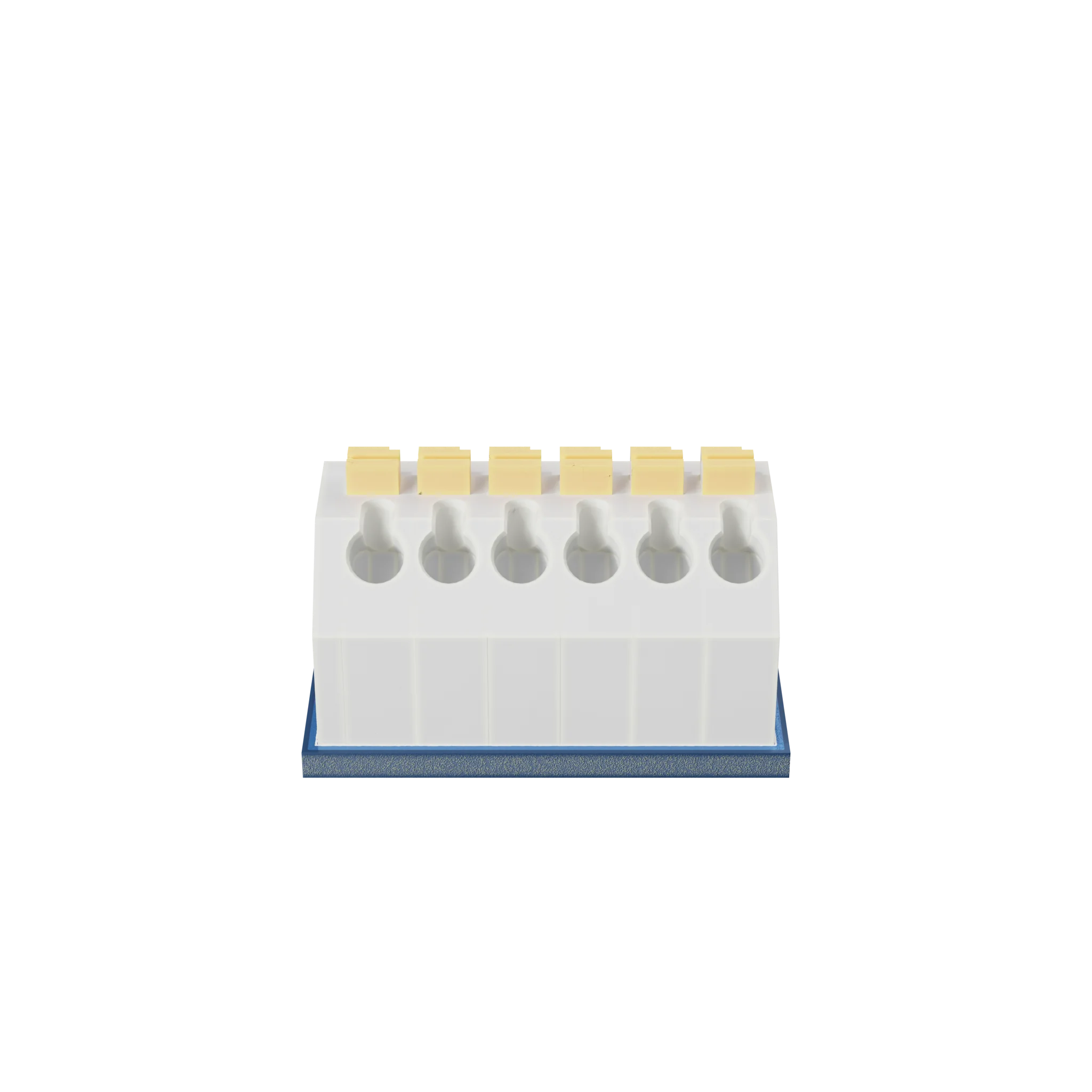

OVERVIEW
Turns Nexor into an SSI encoder reader
Bliss performs no SSI-to-CAN conversion. It is the physical-layer and power interface between the field cable and the carrier. The Nexor carrier generates the clock on its SPI bus, Bliss drives it onto the differential pair, receives the device data and returns it to the carrier, which applies the configuration and publishes the value on the CAN bus. The board runs no firmware of its own and solders onto one face of the carrier through castellated pads.
The supply passthrough is protected by an e-Fuse with a 200 mA current limit, a 37.5 V typical clamp, reverse-polarity protection and a fault flag back to the carrier. The field lines carry TVS suppressors and transceivers rated beyond ±15 kV ESD, and every component is specified from -40°C to +125°C. At power-up the carrier recognizes Bliss through its on-board identification memory. Where the same machine also needs an environmental measurement, the Aeris daughterboard covers it on the opposite face.
01 / Integration
How it works with Nexor
Role split: the module adapts the field lines, the carrier polls and publishes
Bliss Interface
Adapts the field lines and powers the connected device
Nexor CARRIER
Powers, polls the device and publishes on CAN
Resources used on the carrier face
SSI clock SPI clock (SCLK) Carrier clock, driven to the device as a differential RS-422 clock
SSI data SPI data (MISO) Device differential data, received on board and returned to the carrier
Interface enables 2x GPIO Enable or tri-state the clock driver and the data receiver
Sensor-supply control GPIO Switches the device supply on and off (e-Fuse enable)
Fault indication GPIO e-Fuse fault flag: over-current, over-temperature, reverse polarity
Board identification Shared ID bus Identification and configuration memory, address set by the mounting face
Power Node supply, +3.3 V, GND Supplied by the carrier; the board does not use the +5 V rail
02 / Features
Key Features
What makes this module unique
Differential RS-422 signaling: ±200 mV sensitivity, 80 mV hysteresis
Sensor supply protected by an e-Fuse: 200 mA limit, 37.5 V typ. clamp
Open or shorted cable reads as a fail-safe state, with no external bias
Protected field lines: beyond ±15 kV HBM ESD and ±12 kV IEC 61000-4-2
Components specified from -40°C to +125°C, AEC-Q100 ID memory and TVS arrays
03 / Specifications
Technical Specifications
01 · INTERFACE
Signaling
RS-422 differential, as used for SSI
SSI clock
100 kHz - 2 MHz typ. · transceiver up to 50 Mbit/s
Data sensitivity
±200 mV differential, 80 mV hysteresis
Common mode
-7 / +12 V between node and device
Cable length
up to ~100 m at ≤ 1 MHz
Open or shorted line
Steady logic high, fail-safe state
02 · ELECTRICAL
Sensor supply
9 - 28 V, passed through from the node
Current limit
200 mA typ. · latch-off within 0.5 s
Overvoltage clamp
37.5 V typ. (36 - 40 V)
Protection
Reverse polarity to -60 V · IEC 61000-4-4 and -4-5
Field-line ESD
±15 kV HBM · ±12 kV IEC 61000-4-2
03 · PHYSICAL
Dimensions
26 x 28 mm · 4-layer PCB, 1.6 mm
Mounting
16 castellated pads, 2.27 / 3.30 mm pitch
Field connector
6-way, 3.81 mm pitch, optional factory-fit
Temperature
-40 / +125 °C · storage up to +150 °C
Compliance
RoHS · lead-free · AEC-Q100 ID memory and TVS
04 / Applications
Applications
Where it's used
- 01 Encoders
Position and angle from SSI absolute encoders, rotary or linear
- 02 Transducers
Magnetostrictive, draw-wire and inclinometer sensors with SSI output
- 03 Motion control
Position, angle and displacement in motion systems
- 04 Single cable
Remote sensor powered and read over the same field cable
- 05 Harsh environments
Up to +125°C, with lines exposed to noise, ESD and surges
- 06 Dual-function
Two-function CAN node with a second daughterboard
05 / Gallery
Gallery
06 / FAQ
Bliss: Our Customers' Questions
Does Bliss convert SSI to CAN?
Bliss performs no SSI (Synchronous Serial Interface) to CAN conversion: it is the physical-layer and power interface between the field cable and the carrier, and it runs no firmware of its own. The Nexor carrier acts as the SSI master – it generates the clock on its SPI bus, shifts the frame in, applies the device configuration and publishes the value on the CAN bus. Frame length, clock rate, Gray or binary coding, CAN identifiers and update rate are all defined by the carrier firmware, not by this board.
What voltage does an encoder powered by Bliss receive?
The encoder receives the node supply as it is: nothing is regulated on Bliss, the carrier supply passes through an e-Fuse, so the device sees 9-28 V less about 0.1 V dropped across the protection stage at 200 mA. The connected device must therefore accept the installation supply voltage. The current limit is 200 mA typical: beyond it the output is held at the limit and latches off within 0.5 s, raising a fault flag to the carrier.
What happens if the encoder cable is disconnected or shorted?
The Bliss data receiver is internally biased, so an open, shorted or undriven pair reads as a steady logic high instead of noise. The carrier sees the idle state and can report the device as absent rather than publishing a meaningless value on the CAN bus, and no external bias resistors are needed on the field wiring. After an overload the sensor supply stays off until the carrier cycles its enable line.
Should the data pair be terminated on the board or at the encoder?
The clock pair ships terminated with 120 Ω on the board, while the data pair carries the same provision unfitted: termination can then be placed at the device end, where a long run actually needs it. Bliss also tolerates a -7 V to +12 V ground-potential difference between the node and the connected device, and that margin is what makes runs of up to about 100 m at 1 MHz or below practical.
How do Bliss, the carrier and the field cable connect?
Bliss solders onto one face of the Nexor carrier through 16 castellated pads (two side columns of 6 at 2.27 mm pitch and a bottom row of 4 at 3.30 mm), with lead-free reflow soldering to IPC/JEDEC J-STD-020 carried out at Nexilica: the board is delivered already mounted on the node, with no soldering or rework on the user side. The field side carries the two differential pairs, the protected supply and the return on a 6-way, 3.81 mm connector available as a factory-fit option; on the standard build the cable is terminated to the board pads. Wire the field cable with the device unpowered.
GET IN TOUCH
Ready to integrate Bliss?
Need Bliss on your Nexor carrier? Write to us, we reply within 1-2 business days.
Contact Us